Firstly you are going need a board that hosts a AT91SAM7S256 chip and exposes the GPIO in a direct manner i.e. does not have any peripherals attached etc.
Specifically you need to make sure that:
- PA4 - PA10
- PA12 - PA15
- PA24 - PA28
- PA20
- GND
- 3.3V
- nRST
Next you'll need to get hold of a 28 pin DIP socket, preferably the "tulip" kind:
In my case the dev board headers were available as headers with 2 rows of 10 pins:
So I used some crimp connectors and 20 way ribbon cable to connect these up.
Next you'll need to figure out the pin mappings between your dev. board and the pic socket.
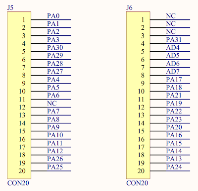
To start you need the schematic for your dev board, mine had this for the pinout info:
Then this must be mapped to the relevant pins on the PIC socket. I used the ARM controller schematics as a guide:
and the PIC mapping:
This should get you to something like this:
From there its just a matter of carefully mapping pin to pin with some wire.
I stripped and tinned the relevant wires in the ribbon cable, pushed them into the mapped holes in the DIP socket and then soldered them in.
The observant reader will notice that GND, 3.3V and nRST are not mapped to the dev board header.
There is another header on my board that provides GND and 3.3V and the JTAG header exposes nRST.
And that is all there is to it :)
HTH
-(e)


